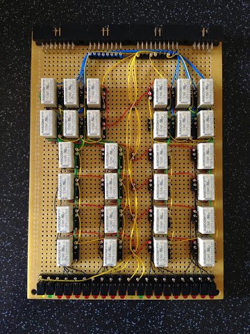
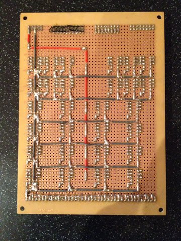
The A/D Register card is now complete and looks like this:


As usual I’ve put a video together that demonstrates this card in operation. This time I don’t show testing the card on its own as the A/D register is pretty much the same as the B/C register shown last time around … needless to say I did test the card fully off camera and everything worked fine (first time believe it or not). As I’ve now got the three ALU cards and four registers I’m finally able to perform multiple operations and accumulate the result. I demonstrate this in the video by performing a series of arithmetic operations by hand.

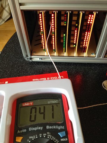
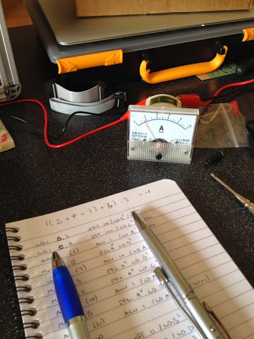
The temperature steadily climbed over a couple of minutes and eventually levelled out at 41 deg C … it’s starting to look a little toasty in there. With the assumption that it’ll be even worse with the enclosure front and back doors on and then worse still when the other three card bays are full I think I’ll need to install some fans in the enclosure to draw the air through. Also of note was how much current was being drawn in this state:

That’s coming in just under 2A … assuming the other remaining cards draw a similar amount I’ll be looking at around 8A total for the lower enclosure. This is the peak current consumption of course so in general use it’ll be much lower. The consumption I’m seeing here is pretty much around where I was expecting but I’ll definitely have to have a quick check around the wiring and make sure everything will be able to take the predicted current levels.
I’m going to take a small break from constructing cards now as I want to make a start on the upper enclosure. This will house the main bus switches, diagnostic display/switches and main display. I’ll blog the design for these in the near future but with all those in place it’ll be much easier to operate the computer when debugging and testing rather than using those fiddly DIP switches.