I’ve covered the construction of the upper and lower memory cards in my last two posts … it’s now time to bring those two cards together to form the memory unit proper and give it all a test.
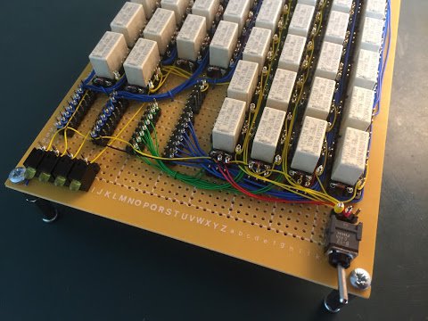
Here’s the upper card (in close up and at a rakish angle) …
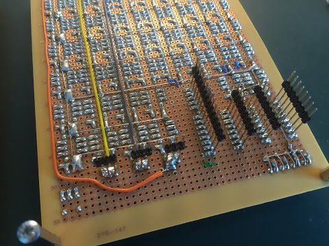
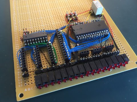
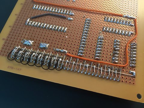
… and here’s the lower memory card (at an equally rakish angle) …
… and when sandwiched together here’s how the memory unit as a whole looks:
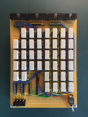
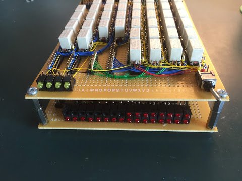
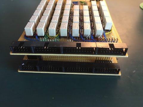
As for all the cards constructed before it I can whip out my trusty breadboard to test the memory unit in isolation before hooking it up to the rest of the computer:
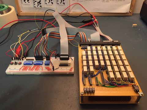
Here I’ve hooked the data bus up to the bar display but it can be switched over to the left hand DIP switches depending on whether I’m reading or setting a value from/to memory. The address bus comes over to the middle and right DIP switches. The eagle eyed of you out there might have noticed that leaves us four bits short of the full address bus but that’s OK for testing purposes. Finally the three switches on the left and wired in to the read, write and B2M (bus to memory) control lines of the Control Y bus.
Anyhoo, it’s video time. Here is an overview of the memory unit, testing it outside of the computer with the breadboard and then finally testing it inside the computer:
With the memory unit complete we’re another step closer to a computer that can step through a program held in memory. The next part of the puzzle is the incrementer which will allow the computer to add one to whatever value is on the address bus and then subsequently place that value back on the address bus. Typically this’ll be used to increment the program counter so it points to the next instruction in memory. Once that’s done we just need to tweak the sequencer and controller and it’s there.