Quite a while ago I decided to give up on the tedious wire wrap technique for building my cards. Although it was certainly more authentic and in-keeping with my computer’s theme it was massively time consuming for me and was ultimately putting me off making progress on construction.
Another problem with my previous construction methods was creating monstrosities like this:
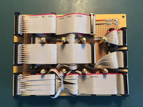
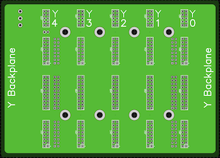
This is the ‘W’ backplane connector which connects five of the ‘W’ type cards together … and its as precarious as it looks and over time I’ve found the ribbon cable on the back of these backplanes are getting a bit temperamental. If left well alone they’re fine but any knocks or pokes and whole lines can become disconnected. To solve this I made my own PCB for the Y backplane removing the need for the ribbon cable:
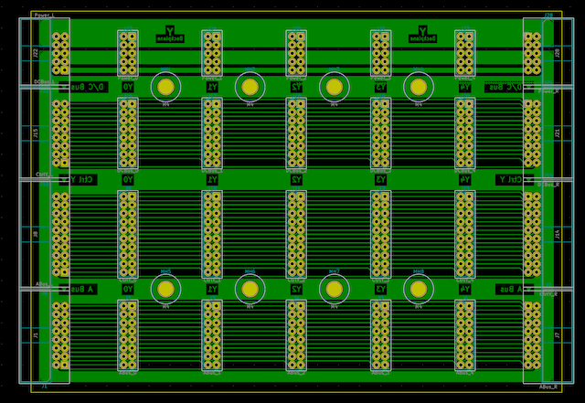
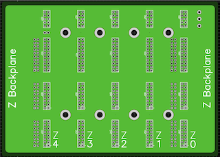
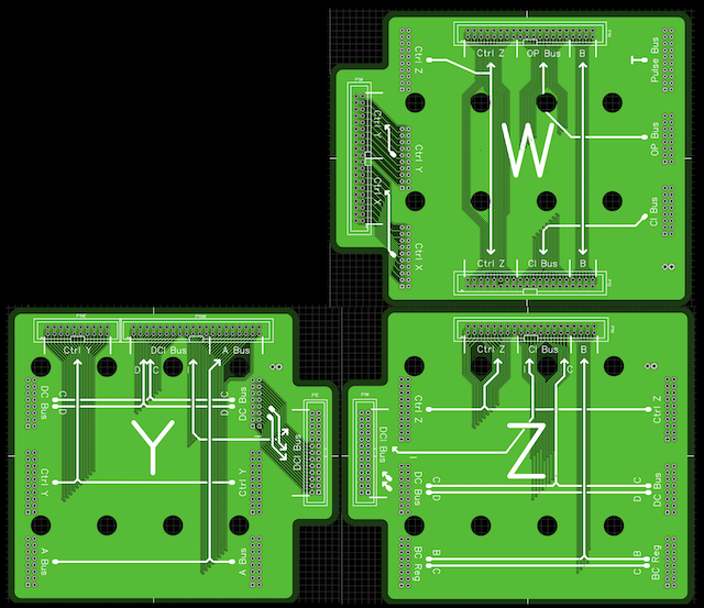
Unsurprisingly then I’m fully intending to replace the remaining backplane cards utilising a similar approach. However, I’m not completely mad … I won’t be making these PCBs by hand and will get a proper PCB company to manufacture these cards instead. As such, I’ve already got the design underway with bays W, Y and Z designed so far:
Now, this is a big step forward in reliability for the backplane cards but there still something I’m not totally happy about:
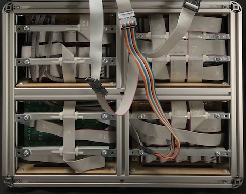
It’s (what I can only describe as) a ’nest’ of ribbon cables. To be fair, this is a photo taken on one of the computer’s ’tidier’ days and more usually there’s cables all over the place and everything is visually chaotic. This is something that’s always bothered me especially when I’m tracking down a fault or need to work around the backplanes.
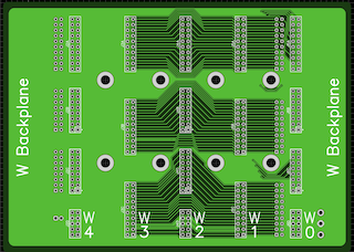
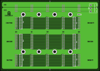
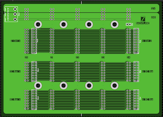
So, the thought process went like this … if I can replace ribbon cables on the backplane itself why can’t I do something similar for the ribbon cables running between the backplanes? … and then it hit me … why not just replace the ribbon cables in that area with another PCB … a ‘daughterboard’ that plugs into the back of each backplane.
Well, yup, there’s designs for those too …
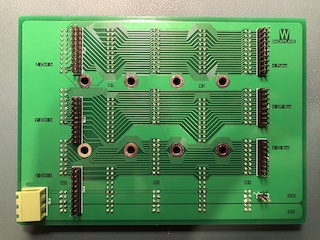
These daughterboards then connect to each other via a single ribbon cable and you can see where the backplane ‘X’ daughter board will go in this pattern at the top left.
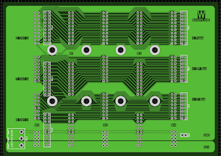
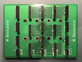
I’m really pleased with the aesthetics of these and, actually, I had the W backplane manufactured a while ago along with a slightly earlier version of the W daughterboard design above. I didn’t get around to blogging about it at the time (that’s now this post) but here’s some pictures:
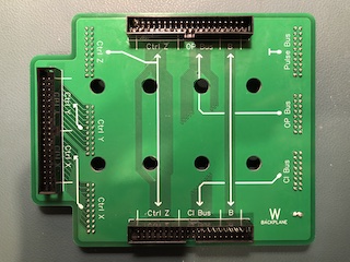
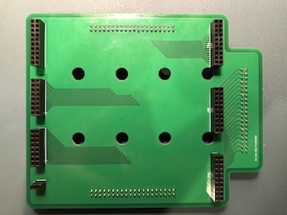
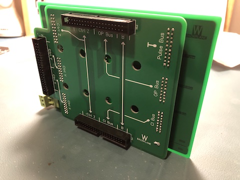
If you’ve been keeping an eye out on my YouTube channel you’ll know I’m nearing the completion of the design for the clock card. Well, as always, these videos are produced quite a bit ahead of the date I publish them so actually I’ve already received the manufactured clock PCB but also received the revised W backplane daughterboard along with the Z and Y backplane/daughterboard pairs. I’ll fit these to the computer in due course and blog or video them if there’s anything of particular note but failing that they’ll just ‘magically’ appear at some point.
If you’d like to take a closer look at any of these you can find the full colour previews in PDF format as follows:
You can also see the schematic for these cards (or even download the Gerber files and manufacture one of your own) at the progress page and cards page.